
High Thermal Conductivity Transfer-Printed Polycrystalline Diamond Membranes for Device- and Chip-Level Thermal Management
Paper details
Section titled “Paper details”| Field | Value |
|---|---|
| Journal | ACS Applied Electronic Materials |
| Published | 2026-06-11 |
| Authors | Husam Walwil, Chenyu Wang, S H Kim, Xuanyu Zhou, Luke Suter |
| DOI | 10.1021/acsaelm.6c00310 |
Removing a 0.87 μm nucleation layer produced a 2.38 μm polycrystalline diamond membrane with an out-of-plane thermal conductivity of 304 ± 82 W m⁻¹ K⁻¹. Its in-plane conductivity was 136 ± 31 W m⁻¹ K⁻¹. Thermal modeling at 6 W mm⁻¹ predicted about 10% lower peak temperature rise for a GaN HEMT with a top-side membrane. The room-temperature membrane interface conductance was only 5.8 MW m⁻² K⁻¹, leaving transfer contact as the main limitation.
Why the nucleation layer controls performance
Section titled “Why the nucleation layer controls performance”Columnar growth produces small grains at the nucleation side and larger grains toward the growth surface. Grain-boundary scattering then suppresses thermal transport, especially in plane. For PCD films below 10 μm, out-of-plane conductivity is typically 3 to 25 times in-plane conductivity.
A prior estimate placed the nucleation region’s thermal resistance at about 9.5 m² K GW⁻¹. That resistance was roughly three times that of the remaining 5.4 μm diamond film. The authors removed this low-quality region before transfer printing. This route also avoids growth-related high-temperature exposure on the device.
Membrane fabrication and surface quality
Section titled “Membrane fabrication and surface quality”About 3.8 μm of PCD was grown on a (100) Si/SiO₂ wafer by microwave plasma-enhanced chemical vapor deposition. Photolithography and electron-beam evaporation formed a Cr/Ni mask with 100 nm Cr and 300 nm Ni. ICP-RIE opened the diamond film and exposed the SiO₂. After mask removal, 49% hydrofluoric acid dissolved the exposed oxide and released the membrane.
The membrane was flipped onto uncured SU-8 on a temporary Si substrate. A second ICP-RIE step removed about 0.87 μm from the nucleation side, leaving a 2.38 μm film. Acetone stripped the SU-8. Two PDMS stamps restored the original growth-side orientation. The membrane was printed onto clean Si without adhesive and annealed at 150 °C for 30 min in N₂.
SEM showed intimate contact without noticeable bending, delamination, or voids. Backside RMS roughness fell from about 34 nm to 11 nm after etching. Raman analysis reduced the estimated sp²/sp³ ratio from about 0.01 to 0.0086. The 1332 cm⁻¹ diamond peak remained after etching.
Conductivity measured by TDTR
Section titled “Conductivity measured by TDTR”TDTR used an approximately 80 nm Al transducer. Pump pulses heated the surface, and a delayed probe tracked the transient response. A multilayer heat-diffusion model fitted the measured signal ratio.
Large pump and probe spots of about 27 and 15 μm measured out-of-plane conductivity at 7, 10, and 12 MHz. Smaller spots of about 7.5 and 5 μm measured in-plane conductivity at 7 and 10 MHz.
The nucleation-free membrane was measured from the growth side. The as-grown reference was measured from the nucleation side.
| Sample and method | Thickness | Out-of-plane κ, W m⁻¹ K⁻¹ | In-plane κ, W m⁻¹ K⁻¹ |
|---|---|---|---|
| Nucleation-free PCDm, TDTR | 2.38 μm | 304 ± 82 | 136 ± 31 |
| As-grown PCDm with nucleation region, TDTR | 3.25 μm | 187 ± 41 | 103 ± 17 |
| Nucleation region, two-layer fit | 0.87 μm | 48 ± 3.8 | 49.5 ± 19 |
Removal increased the effective in-plane conductivity by about 25%. The anisotropy ratio rose from about 1.82 to 2.2 because out-of-plane transport benefited more strongly. The 2.38 μm membrane exceeded several reported out-of-plane values for similar or greater thickness films that retained their nucleation regions. Its conductivity still fell below the typical 800 to 1500 W m⁻¹ K⁻¹ of 10 to 100 μm PCD films and bulk single-crystal diamond above 2000 W m⁻¹ K⁻¹.
Depth uniformity and temperature response
Section titled “Depth uniformity and temperature response”TDTR frequency varied the thermal probing depth. The 2.38 μm membrane showed negligible variation in either conductivity over its thickness. A second membrane, etched by 0.98 μm to 2.27 μm, gave nearly identical results. SEM grain sizes were about 1.16 μm and 1.17 μm for the two membranes. The authors concluded that the nucleation region had been fully removed.
The unetched 3.25 μm membrane showed strong depth dependence in both conductivity and anisotropy. Transport within its nucleation region was nearly isotropic, while the full membrane was anisotropic. This result identifies the nucleation region as a separate thermal layer.
Both conductivities decreased between 300 K and 450 K. The in-plane value followed about T⁻⁰·³, while the out-of-plane value followed about T⁻¹·⁰. The authors interpreted the weaker in-plane temperature dependence as evidence that grain-boundary scattering dominated. They associated the stronger out-of-plane dependence with intrinsic phonon Umklapp scattering.
Transfer interface limits heat flow
Section titled “Transfer interface limits heat flow”The PCDm/Si conductance was extracted with a dual-frequency TDTR ratio. The frequency pair was 1 and 7 MHz at room temperature and 1 and 3 MHz at elevated temperatures.
The interface had a room-temperature thermal boundary conductance, G2, of 5.8 MW m⁻² K⁻¹. This was about 11% of the typical 50 MW m⁻² K⁻¹ for directly grown PCD on Si. It was also 1.7% of the calculated 350 MW m⁻² K⁻¹ for a perfect PCD/Si interface.
The authors attributed the low conductance to incomplete contact, weak bonding, and 11 nm surface roughness. A cited transfer-printing study reported true contact areas of 10 to 15% for thin metal films. Reported conductance for transfer-printed films usually ranged from 10 to 65 MW m⁻² K⁻¹.
Residual PDMS was considered as a possible cause. The measured Al/PCDm conductance, G1, was 140 ± 11.5 MW m⁻² K⁻¹. A 5 nm PDMS layer with conductivity 0.1 W m⁻¹ K⁻¹ would produce an effective conductance near 20 MW m⁻² K⁻¹. The authors therefore ruled out residual PDMS as the main cause.
Interface conductance increased nearly linearly with temperature. The authors associated this trend with inelastic phonon transmission, consistent with their molecular dynamics comparison.
GaN HEMT cooling model
Section titled “GaN HEMT cooling model”The thermal model was validated against a single-finger GaN-on-Si HEMT using multispectral Raman thermometry. The device had a 200 μm gate width, 23.5 μm channel length, 6 μm gate length, and 14 μm drain-to-gate spacing. It used a 625 μm Si substrate. Raman shifts of the GaN E₂(high) and A₁(LO) modes tracked lattice temperature. A COMSOL model reproduced the measured temperature rise.
At 6 W mm⁻¹, the model predicted that a top-side 2.38 μm membrane lowered peak temperature rise by about 10%. This case used the measured interface conductance and an effective PCDm/GaN thermal boundary resistance of 287 m² K GW⁻¹. A 2.38 μm model membrane containing a 0.87 μm nucleation layer and 1.51 μm high-conductivity layer produced only a 7.5% reduction.
The authors also tested lower interface resistances. Assuming a PCDm/Si resistance of 16 m² K GW⁻¹ gave an effective PCDm/GaN resistance of 131 m² K GW⁻¹ and a 12% reduction. At 3.1 m² K GW⁻¹, the effective resistance reached 118 m² K GW⁻¹. The nucleation-free case then reduced peak temperature rise by 12.5%, compared with 9% for the case containing a nucleation region.
These cooling results are model predictions for hypothetical top-side integration. The study did not report an experiment on a HEMT with a transferred PCDm heat spreader.
Material selection criteria
Section titled “Material selection criteria”Film thickness alone is a poor predictor of thin PCD heat-spreader performance. The nucleation side must be dense and free of low-conductivity material before transfer. Device engineers must also treat interface conductance as a separate design variable because low G2 can offset high membrane conductivity.
The results also depend on growth conditions, grain-size distribution, grain-boundary density, and grain orientation. The TDTR uncertainty analysis assigned 10% uncertainty to Al conductivity and G1, and 3% to layer thickness and laser spot size. For the reported stack, 5.8 MW m⁻² K⁻¹ remains the measured interface limit, while the 10% cooling result remains a model prediction.
Materials and support
Section titled “Materials and support”The GaN HEMT and 3D chip heat-spreader application requires MPCVD-grown polycrystalline diamond in a thin, transferable form with a dense nucleation-side surface. 6CCVD offers MPCVD-grown polycrystalline diamond with thickness from 0.1 to 500 micrometers, which includes the 2.38 micrometer thickness used in the paper. The diamond materials catalog shows the available forms, while engineering support can review etch, transfer, and bonding requirements.
View Original Abstract
High Resolution Image Download MS PowerPoint Slide The thermal conductivity of polycrystalline diamond (PCD) thin films can vary by more than an order of magnitude due to differences in the microstructure. PCD films often undergo columnar growth where the grain size increases with the film thickness. Therefore, phonon-grain boundary scattering significantly impacts the thermal conductivity and interfacial thermal transport. In this work, to utilize PCD membranes (PCDm) as transfer-printed heat spreaders for high-power electronic devices and chiplets, a fabrication process was developed where the defective and low thermal conductivity nucleation region of the PCD film is removed to form a high-thermal-conductivity membrane. The temperature-dependent anisotropic thermal conductivity of a ∼2.4 μm-thick PCDm (with the nucleation region removed) and the thermal boundary conductance (TBC) across the PCDm/Si interface were characterized via time-domain thermoreflectance (TDTR). The measured out-of-plane ( κ out = 304 ± 82 W m −1 K −1 ) and in-plane thermal conductivities ( κ in = 136 ± 31 W m −1 K −1 ) of the nucleation region-free membrane are significantly higher than those ( κ out = 187 ± 41 and κ in = 103 ± 17 W m −1 K −1 ) for an as-grown ∼3.3 μm-thick PCDm that includes the nucleation region. The measured interfacial TBC at the PCDm/Si interface was determined to be 5.8 MW m -2 K −1, which is lower than typical values for PCD films directly grown on Si. Thermal modeling of a single-finger GaN high electron mobility transistor (HEMT) shows that a top-side integrated PCDm reduces the channel peak temperature by ∼10%. Simulation results suggest that the high-thermal-conductivity PCDm can serve as effective means for the cooling of high-power electronic devices and 3D-integrated circuits if the TBC is improved via optimization of the transfer-printing process.

Electronic Grade Intrinsic Diamond Epitaxial Wafer H Terminated Superior 100 Mosfet Ready Substrate
View Specs →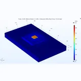
Advanced Thermal Simulation Service Diamond Heat Spreader Performance Analysis
View Specs →
Free Standing Polycrystalline Cvd Diamond Membrane
View Specs →References we cover
Section titled “References we cover”- Schottky Barrier Diodes Based on Freestanding Polycrystalline Diamond Membranes
- Mechanical and Electrical Properties of Free‐standing Polycrystal Diamond Membranes
- Record-Low Thermal Boundary Resistance between Diamond and GaN-on-SiC for Enabling Radiofrequency Device Cooling
- Tunable Thermal Energy Transport across Diamond Membranes and Diamond-Si Interfaces by Nanoscale Graphoepitaxy
- Direct Visualization of Thermal Conductivity Suppression Due to Enhanced Phonon Scattering Near Individual Grain Boundaries