
Description
Advanced Diamond Epitaxial Growth Service for Next-Generation Electronics
Our Diamond Epitaxial Growth Service offers a pathway for researchers and engineers to overcome the limitations of traditional silicon-based semiconductors. As power density, operating frequency, and harsh-environment demands increase, materials like diamond are essential for technological advancement. By leveraging diamond’s exceptional properties as a wide-bandgap semiconductor, this service enables the creation of devices with unparalleled performance.
We utilize state-of-the-art Microwave Plasma Chemical Vapor Deposition (MPCVD) technology to grow multiple, distinct epitaxial layers on a pristine single-crystal diamond substrate. This atomic-level precision allows for the fabrication of complex device structures, turning your theoretical designs into tangible, high-performance components.
Customized Multi-Layer Structures
While every project is custom-tailored, we can produce complex structures designed for specific device functionalities. The following is a representative configuration for a power device:
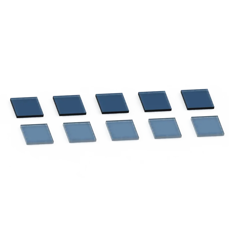
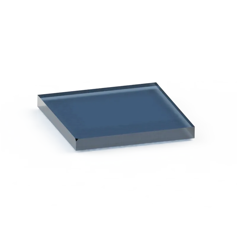
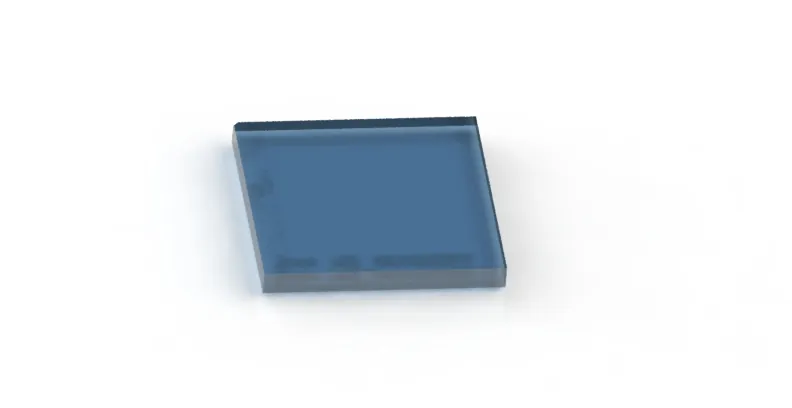
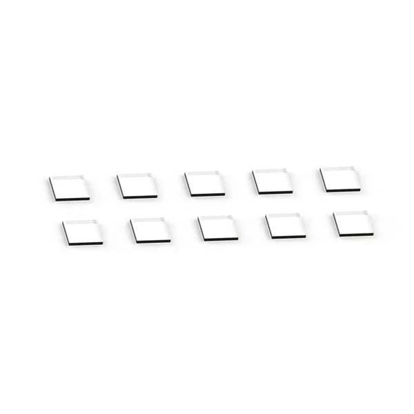
- Substrate: High-Purity Undoped Single-Crystal Diamond (SCD) Plate (e.g., 5 x 5 x 0.3 mm)
- Layer 1 (Drift Layer): Lightly Boron-Doped (p⁻) layer, 2 µm thickness, with a doping concentration of 1016 – 1017 cm⁻³
- Layer 2 (Contact Layer): Heavily Boron-Doped (p⁺) layer, 100-200 nm thickness, with a doping concentration of 1019 – 1020 cm⁻³
Our team works directly with you to define the exact layer thicknesses, doping profiles, and substrate dimensions required for your project.
Key Features & Technical Benefits
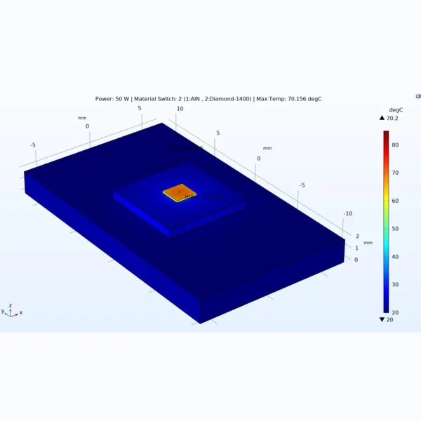
- Superior Thermal Management: Built upon a substrate with a thermal conductivity exceeding 2200 W/m·K, our epitaxial wafers efficiently dissipate heat, enabling higher power densities and enhanced device reliability.
- Precise Doping Control: We precisely control the incorporation of boron to achieve specific electronic properties, creating distinct p- and p+ layers essential for modern device architectures.
- Atomic-Level Smoothness: Wafers are delivered with an epi-ready surface polish (Ra < 1nm), providing a flawless interface for subsequent photolithography, metallization, and device fabrication steps.
- High Breakdown Voltage: The wide bandgap of diamond facilitates the design of devices capable of withstanding much higher electric fields than silicon or silicon carbide, leading to smaller and more efficient components.
Applications for our Diamond Epitaxial Growth Service
This custom service is engineered for the most demanding applications in electronics and research:
- High-Power & High-Frequency MOSFETs: Create field-effect transistors for power converters, electric vehicle systems, and RF power amplifiers that operate more efficiently and at higher temperatures. Our service is the custom pathway for products like our standard Diamond Epitaxial Wafer for MOSFETs.
- Advanced Diodes: Fabricate Schottky and PiN diodes for high-power rectifiers and high-frequency applications, benefiting from diamond’s low reverse leakage current and fast switching speeds.
- Quantum Computing & Sensing: Develop nitrogen-vacancy (NV) center-based quantum sensors and computing components that require precisely engineered material properties and an ultra-pure crystal environment.
- Radiation-Hard Electronics: Build detectors and electronics for aerospace, defense, and high-energy physics applications where devices must remain operational in extreme radiation environments.
How to Initiate a Project
- Submit Your Specifications: Use our website’s contact form to detail your desired layer structure. Please include substrate dimensions, number of layers, thickness of each layer, and the boron doping concentration for each layer.
- Technical Consultation: Our PhD engineering team will meticulously review your request. We may schedule a brief consultation to confirm technical details and discuss project feasibility to ensure optimal results.
- Formal Quotation: Following the consultation, we will provide a comprehensive, formal quote for your custom epitaxial growth project, which will include the projected lead time and shipping details.
Reviews
There are no reviews yet.