Description
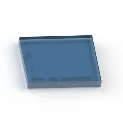
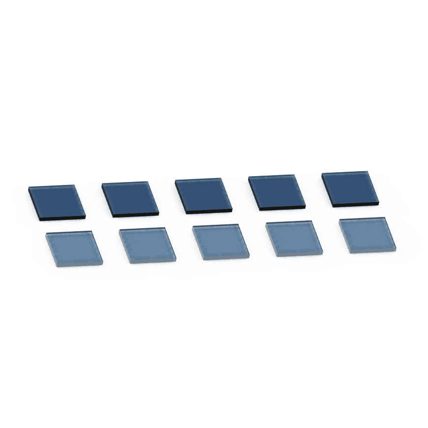
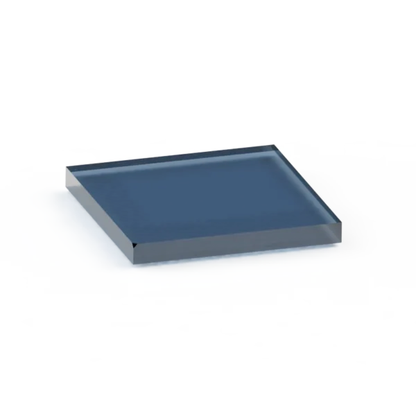
Diamond Epitaxial Wafer for Diodes: The Ultimate Solution for High-Power Applications
Are you searching for a reliable, high-performance diamond epitaxial wafer for diodes? Look no further! Our Diamond Epitaxial Wafer is engineered to meet the demands of advanced semiconductor devices, offering unparalleled thermal conductivity, durability, and efficiency. Whether you’re working on high-power diodes or cutting-edge electronics, this wafer is your go-to solution.
Table of Contents
Specifications
| Parameter | Value |
|---|---|
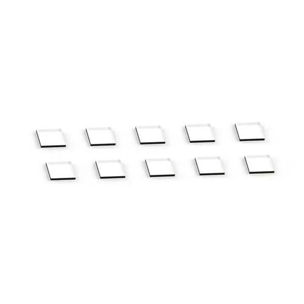
| Base Undoped Diamond Layer | 500 ± 50 µm |
| Diamond Type | Single Crystal Diamond (SCD) |
| Heavily Boron-Doped Diamond Layer | ~2 µm |
| Dimension | 5 x 5 mm |
Key Features
- High Thermal Conductivity: Diamond’s exceptional thermal properties ensure efficient heat dissipation, making it ideal for high-power devices.
- Superior Electrical Performance: The boron-doped diamond layer enhances conductivity, enabling high-current applications.
- Robust and Durable: Single Crystal Diamond (SCD) ensures long-term reliability even in harsh environments.
- Precision Engineering: Each wafer is crafted to exact specifications, ensuring consistency and performance.
Applications
Our Diamond Epitaxial Wafer is versatile and finds use in a wide range of applications, including:
- High-power diodes and rectifiers
- Advanced semiconductor devices
- Quantum computing components
- High-frequency electronics
- Thermal management systems
- Optoelectronics
- Radiation-hardened devices
- Energy-efficient power modules
Benefits
- Enhanced Efficiency: The combination of undoped and boron-doped layers ensures optimal performance in high-power scenarios.
- Cost-Effective: Despite its advanced properties, our wafer is competitively priced, offering excellent value for money.
- Quick Turnaround: With a standard lead time of just 1 month, you can start your projects without delay.
FAQs
1. What is the advantage of using Single Crystal Diamond (SCD)?
SCD offers superior thermal and electrical properties compared to polycrystalline diamond, making it ideal for high-performance applications.
2. Can I customize the dimensions of the wafer?
Yes, we offer customization options. Contact us for more details.
3. How does the boron-doped layer enhance performance?
The boron-doped layer improves electrical conductivity, enabling the wafer to handle higher currents efficiently.
4. What is the lead time for this product?
The standard lead time is 1 month, but expedited options are available upon request.
Why Choose Us?
We specialize in providing high-quality diamond wafers tailored to your needs. Our products are backed by extensive research and development, ensuring you get the best performance for your applications. Check out our related products like the Diamond Epitaxial Wafer for MOSFET and the Boron-Doped Diamond Plate for more options.
External Resources
For more insights into diamond-based semiconductor applications, check out these resources:
- A Review of Diamond Materials and Applications in Power Semiconductor Devices
- Diamond Semiconductor Devices: State-of-the-Art of Material Growth and Device Processing
- Diamond Wafer Technology, Epitaxial Growth, and Device Processing
Ready to elevate your projects with our Diamond Epitaxial Wafer for Diodes? Buy now and experience the difference!

Reviews
There are no reviews yet.