
Description
Table of Contents
- Introduction to the Electronic Grade Intrinsic Diamond Epitaxial Wafer (H-Terminated)
- Why You Need Our Electronic Grade Intrinsic Diamond Epitaxial Wafer (H-Terminated)
- Overcoming Substrate Bottlenecks
- Real-World Applications
- Technical Specifications
- External Scientific Resources on Diamond Electronics
- FAQs
Introduction to the Electronic Grade Intrinsic Diamond Epitaxial Wafer (H-Terminated)
When engineering advanced power electronics, choosing the correct Electronic Grade Intrinsic Diamond Epitaxial Wafer (H-Terminated) solves the critical problem of subsurface damage and uncontrolled surface scattering. We observe many researchers procuring standard mechanical grade plates, assuming they are smooth enough for device fabrication. That oversight results in trapped charges, poor channel mobility, and wasted laboratory time. We engineered this high-purity product to bridge this gap for the scientific community.
By strictly managing the microwave plasma chemical vapor deposition (MPCVD) process, we deliver this advanced substrate ready for immediate active channel fabrication. You get a perfect crystal lattice straight out of the vacuum seal. We do the heavy lifting in surface preparation so your team can focus on fabricating high-performance field-effect transistors and quantum devices. Producing an electronic grade interface demands absolute precision. We strictly regulate the methane and hydrogen plasma ratios during the MPCVD growth cycle to guarantee the exact electrical properties you need.
Why You Need Our Electronic Grade Intrinsic Diamond Epitaxial Wafer (H-Terminated)
The core performance of this material relies on a highly controlled step-flow growth mode. We start by applying a rigorous fine polishing process on the base single crystal diamond to achieve an atomic-scale smoothness of Ra < 1 nm. Standard mechanical polishing leaves amorphous carbon and micro-scratches beneath the surface. The step-flow epitaxy replicates the flawless underlying lattice.
We continuously monitor the plasma temperature to prevent any non-diamond carbon sp2 bonds from forming in the epi layer.
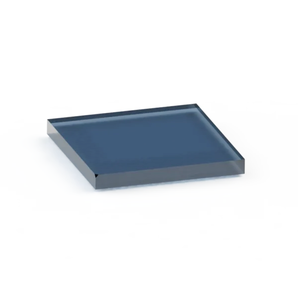
By keeping the growth purely in the step-flow regime, we eliminate step-bunching and hillock formation entirely. The top epitaxial layer on the Electronic Grade Intrinsic Diamond Epitaxial Wafer (H-Terminated), which runs 200 nm to 500 nm thick, remains absolutely intrinsic. We keep nitrogen impurity levels strictly below 1 ppb. This purity prevents deep trap levels from compensating your charge carriers or reducing channel mobility.
Overcoming Substrate Bottlenecks
We know the pain of running an expensive semiconductor fabrication process only to find out your starting wafer had hidden polishing lines or subsurface damage. When you use our homoepitaxial substrate, you bypass these hidden defects completely. The pristine, as-grown epi layer provides an untouched crystal lattice interface for your gate dielectrics.
We finish the production cycle with an in-situ hydrogen plasma treatment. The “As-Grown” hydrogen termination creates a two-dimensional hole gas (2DHG) on the surface via transfer doping. This termination acts as a highly conductive p-type channel, usually reaching sheet carrier concentrations around 1E13 cm-2, with absolutely no need for complex or destructive ion implantation. Your Electronic Grade Intrinsic Diamond Epitaxial Wafer (H-Terminated) arrives packaged in vacuum-sealed Gel-Pak or Fluoroware containers. We block surface oxidation during transit, preserving the delicate, conductive H-termination. If your research group requires an insulating surface instead, we can apply an oxygen termination prior to shipment upon request.
Real-World Applications for the Electronic Grade Intrinsic Diamond Epitaxial Wafer (H-Terminated)
We see clients across global research facilities integrating our materials into cutting-edge systems. This material excels in these ten practical applications:
- Diamond MOSFETs: Building lateral and vertical transistors using the 2DHG conductive channel. The high carrier mobility allows for extreme power density without thermal breakdown.
- Diamond MESFETs: High-frequency switches requiring minimal gate leakage. The intrinsic layer ensures parasitic currents stay near absolute zero.
- Quantum Sensing: Hosting near-surface NV centers where low nitrogen background (under 1 ppb) is mandatory. The pristine lattice extends the spin coherence times of the quantum states.
- High-Frequency RF Devices: Taking advantage of the extreme thermal conductivity and high breakdown fields to amplify signals in radar and satellite communications.
- Deep-Depletion Transistors: Managing high-voltage power switching in extreme environments, outperforming standard silicon carbide substrates.
- High-Temperature CMOS Inverters: Pairing p-channel diamond FETs with n-channel GaN HEMTs for logic circuits operating past 350 Celsius. This hybrid approach enables entirely new classes of high-heat electronics.
- Spin-Based Quantum Computing: Providing a defect-free lattice for quantum state preservation.
- Electrochemical Sensors: Utilizing the wide potential window of the diamond surface for extreme accuracy.
- Radiation-Hardened Detectors: Deploying sensors in aerospace or nuclear facilities where standard silicon heavily degrades.
- Solid-State Biosensors: Leveraging the pH sensitivity of the 2DHG layer for bio-molecule detection.
Technical Specifications
We maintain strict quality control to guarantee the performance of every wafer. Review the standard parameters below.
| Parameter | Specification |
|---|---|
| Product Name | Electronic Grade Intrinsic Diamond Epitaxial Wafer (H-Terminated) |
| Technology | MPCVD Diamond Standard |
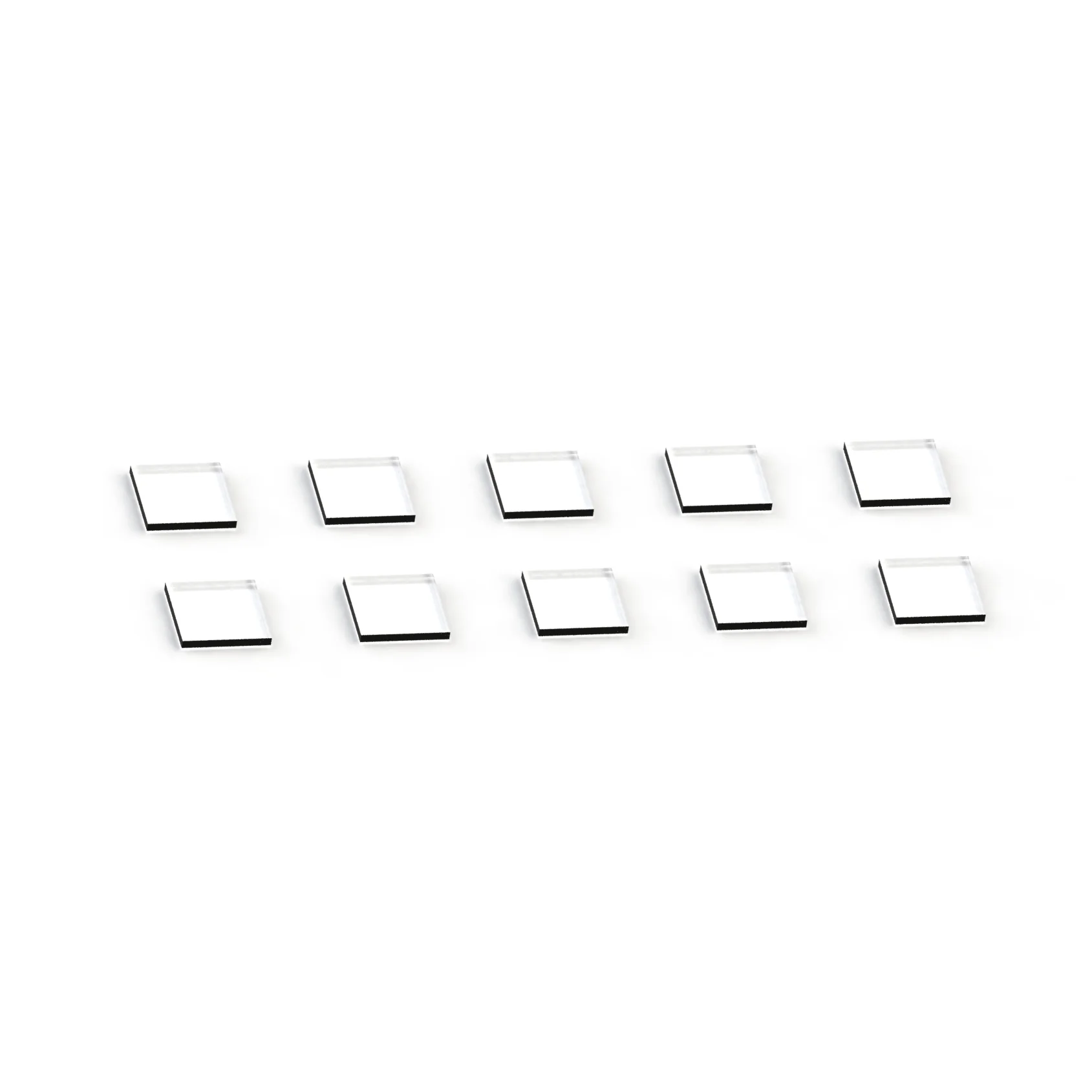
| Substrate Dimensions | 3×3 mm, 5×5 mm, 10×10 mm |
| Epitaxial Layer Thickness | 200 nm to 500 nm |
| Doping Concentration | Intrinsic / Undoped |
| Surface Roughness (Ra) | < 1 nm |
| Surface Termination | Hydrogen (Conductive 2DHG) or Oxygen (Insulating) |
| Packaging | Vacuum-sealed Gel-Pak |
| Standard Lead Time | 1 month unless otherwise stated |
External Scientific Resources on Diamond Electronics
We base our manufacturing processes on rigorous, validated scientific research. You can verify the data on diamond epitaxy and 2DHG properties through these live, peer-reviewed sources:
- Materials (MDPI): The Influence of Process Parameters on Hydrogen-Terminated Diamond (2025)
- IEEE Xplore: Hydrogen-terminated diamond FET and GaN HEMT delivering CMOS inverter operation (2020)
- PubMed Central: A Review of Diamond Materials and Applications in Power Semiconductor Devices (2024)
- Applied Physics Letters: Enhancement to the conductivity of surface transfer-doped (111) diamond (2025)
- Materials (MDPI): A High-Performance All-Carbon Diamond Pixel Solar-Blind Detector (2025)
- IEEE Trans. Electron Devices: High output power density of 2DHG Diamond MOSFETs (2021)
- ANR: Large Size Diamond MOSFET (LSD-MOSFET) Project
FAQs about the Electronic Grade Intrinsic Diamond Epitaxial Wafer (H-Terminated)
Q1: Can we adjust the epitaxial layer thickness of the Electronic Grade Intrinsic Diamond Epitaxial Wafer (H-Terminated)?
A1: Yes. We standardly grow layers between 200 nm and 500 nm, but we readily accept customized requests for thicker layers. You can review our Customization Services for advanced multi-layer builds and custom quoting.
Q2: How does the hydrogen termination remain stable?
A2: We vacuum-seal the wafer right after the plasma treatment inside our cleanroom. The 2DHG stays active as long as you prevent high-temperature atmospheric oxidation during your unboxing and subsequent processing steps.
Q3: Is this product different from a standard single crystal plate?
A3: Absolutely. A standard Single Crystal CVD Diamond Plate acts as an excellent mechanical substrate for thermal spreaders or optical windows. For active FETs, you need the low-defect step-flow epitaxy we provide here. If you need a larger, cost-effective base purely for thermal management, consider our Polycrystalline CVD Diamond Wafer. If your project involves heavy boron integration, review our Diamond Epitaxial Wafer for Diodes.
Q4: Do you offer metalization for source and drain contacts?
A4: Yes. While the standard product ships with an as-grown H-terminated surface, we provide custom metalization services as a Non-Recurring Engineering (NRE) request. We regularly work with Tungsten, Platinum, Palladium, Silver, and Gold. We have also internally tested Copper metalization. Contact us with your specific masking requirements for a detailed engineering review.
Q5: What are the shipping terms for these sensitive substrates?
A5: We ship all electronic grade materials under strict vacuum-sealed conditions. By default, we provide DDU (Delivered Duty Unpaid) shipping. If you need a DDP (Delivered Duty Paid) quote, simply provide your recipient contact details and Tax ID when submitting your inquiry. We coordinate with standard global couriers to ensure the package arrives without thermal or physical shock.


Reviews
There are no reviews yet.