
Your cart is currently empty!
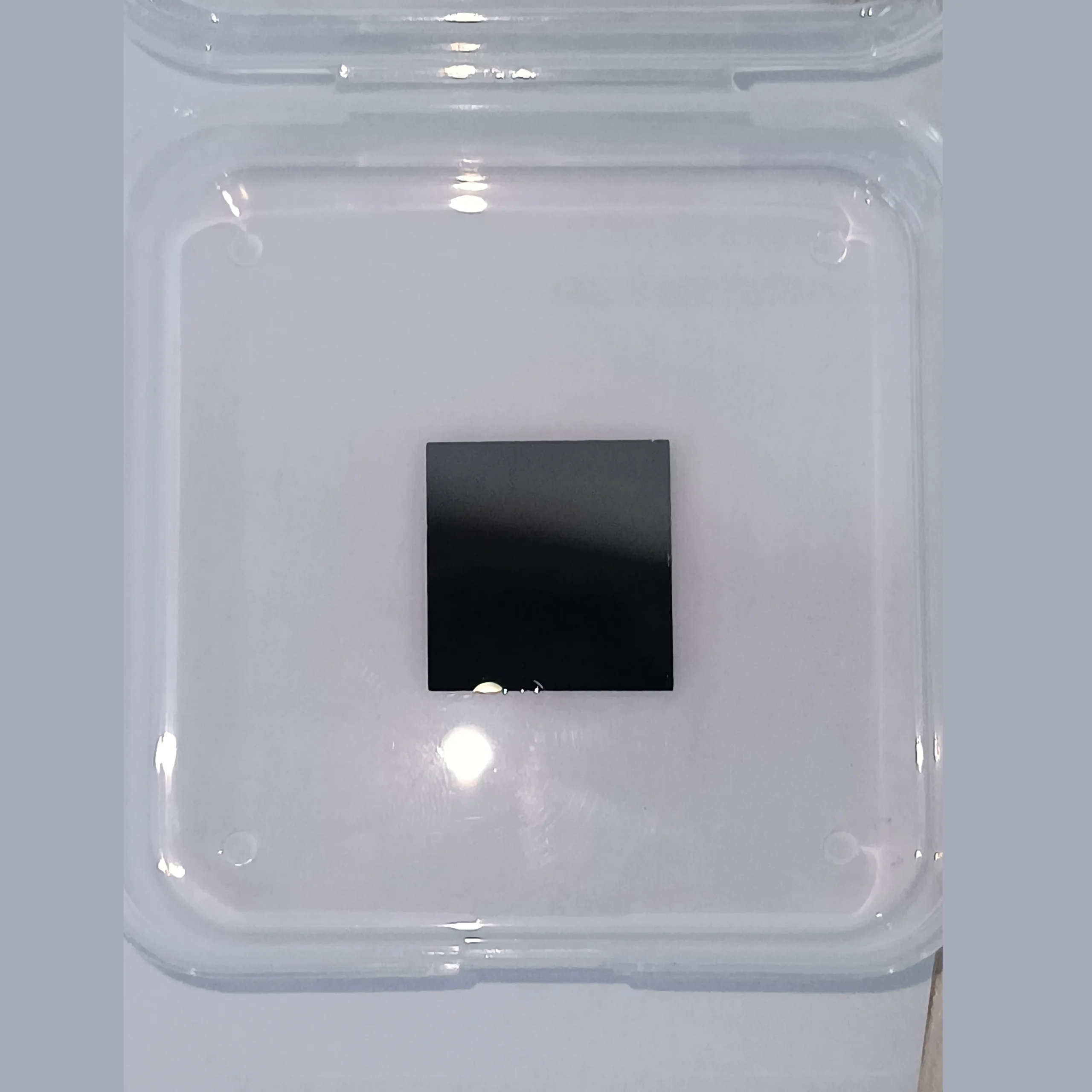
Free-Standing Boron-Doped Polycrystalline Diamond Film
Product successfully added to the Quote List
Description
Our Free-Standing Boron-Doped Polycrystalline Diamond Film is the answer for engineers and researchers pushing the boundaries of modern electronics. If you’re struggling with the thermal limits of silicon, the high costs of single-crystal diamond, or the performance bottlenecks in high-power devices, you’ve found your solution. This material offers a robust, high-performance foundation for your most advanced heterojunction-based projects, moving beyond the constraints of conventional substrates.
Table of Contents
- Why Our Free-Standing Boron Doped Polycrystalline Diamond Film is a Game-Changer
- Core Features at a Glance
- Technical Specifications
- Unlocking Next-Generation Applications with BDD Film
- Frequently Asked Questions
Why Our Free-Standing Boron Doped Polycrystalline Diamond Film is a Game-Changer
We craft each film using a state-of-the-art Microwave Plasma Chemical Vapor Deposition (MPCVD) process, which allows for unparalleled control.
This isn’t just any diamond; it’s a material precisely engineered for semiconductor applications.
By introducing boron during the growth phase, we transform diamond from a supreme insulator into a highly effective p-type semiconductor.
This p-type conductivity is fundamental for creating the high-performance p-n heterojunctions that form the core of so many electronic devices.
Unlike substrates that are just a coating, our films are ‘free-standing.’
This means they are fully self-supporting wafers, giving you complete design freedom for integration.
The final product is a Free-Standing Boron Doped Polycrystalline Diamond Film with a combination of properties you simply can’t find elsewhere: massive thermal conductivity, precisely controlled electrical resistivity, and the legendary hardness of diamond.
Its structure and properties make it an ideal candidate for forming heterojunctions with other materials, a topic explored in studies like this analysis of nanocrystalline diamond/silicon heterojunctions.
Core Features at a Glance
- Exceptional Thermal Management: With thermal conductivity over 1500 W/(m·K), it dissipates heat far more efficiently than copper or any other metal, ensuring your devices run cooler, last longer, and perform reliably under load.
- Tailored P-Type Conductivity: We precisely control the boron doping concentration (from ~E17 to ~E20 atoms/cm³), resulting in a finely tuned resistivity of 2-24 mΩ·cm. This is perfect for creating efficient diamond heterojunction diodes and other semiconductor structures.
- Pristine Surface for Fabrication: One side is polished to an incredible surface roughness of Ra ~1nm. This ultra-smooth surface is essential for epitaxial growth and creating high-quality, low-defect interfaces in your devices.
- Robust and Versatile: Available in diameters from 1mm to 100mm and thicknesses from 1µm to 10µm, these self-supporting films offer maximum versatility for a wide range of device architectures.
- Engineered for Extreme Environments: Diamond’s ultra-wide bandgap (5.47 eV) makes it naturally suited for high-power, high-frequency, and high-temperature applications where traditional materials would degrade or fail.
Technical Specifications
| Property | Specification |
| Material | Boron-Doped Polycrystalline Diamond (BDD) |
| Growth Method | Microwave Plasma Chemical Vapor Deposition (MPCVD) |
| Diameter | 1 – 100 mm |
| Thickness | 1 – 10 µm |
| Thermal Conductivity | >1500 W/(m·K) |
| Resistivity | 2 – 24 mΩ·cm |
| Boron Concentration | ~1017 to ~1020 atoms/cm³ |
| Surface Roughness | One Side Ra ~1nm, other side ~30-500nm (thickness dependent) |
Unlocking Next-Generation Applications with BDD Film
Our Free-Standing Boron Doped Polycrystalline Diamond Film isn’t just a material; it’s a key that unlocks innovation across multiple industries. Its unique combination of properties is driving breakthroughs where performance and reliability are critical. Researchers are actively exploring its potential, as highlighted in comprehensive reviews on diamond-based heterojunctions.
Here are just a few areas where these films are making a difference:
- High-Power and High-Frequency Electronics: Build next-generation transistors and diodes capable of handling higher voltages and switching at faster frequencies. The exceptional thermal conductivity is crucial for managing heat, a primary failure point in GaN and SiC devices. This is especially true when creating heterojunctions with other wide-bandgap materials like β-Ga2O3.
- Optoelectronics: The film’s properties are perfect for high-performance UV LEDs and detectors. Forming heterojunctions with one-dimensional metal oxides such as ZnO or TiO2 creates new avenues for advanced photodetector technologies.
- Radiation Detectors: Diamond is inherently radiation-hard, making it a superior material for detectors in high-energy physics, medical imaging, and space exploration. A Free-Standing Boron Doped Polycrystalline Diamond Film offers a scalable and robust alternative to silicon-based detectors.
- Quantum Technologies: While our quantum-grade single-crystal diamonds are the go-to for qubit applications, these polycrystalline films serve as excellent substrates and components in developing the surrounding quantum device architecture.
- Advanced Electrochemistry: BDD electrodes are prized for their wide electrochemical window, low background current, and extreme resistance to fouling and corrosion. They are ideal for water treatment, electro-synthesis, and highly sensitive electrochemical sensors.
- Thermal Management Substrates: Use the film as an ultra-high-performance diamond heat spreader, directly bonded to active semiconductor wafers using innovative techniques like surface activated bonding for superior thermal contact.
Frequently Asked Questions
What is the primary advantage of a ‘free-standing’ film?
A free-standing film is a self-supporting diamond wafer, not a thin layer on a substrate like silicon. This gives you incredible design and integration flexibility. You can use it as a primary substrate for growing other materials (like GaN), bond it into complex device stacks, or use it on its own. This approach eliminates the property mismatches and constraints imposed by a non-diamond host substrate.
Why is this Free-Standing Boron Doped Polycrystalline Diamond Film made with MPCVD?
Microwave Plasma Chemical Vapor Deposition (MPCVD) is the leading technology for growing high-quality diamond. It gives us precise, atomic-level control over the growth environment. This means we can ensure high purity, accurately control the boron doping levels, and produce films with excellent crystal structure and uniformity over large areas. This process is essential for achieving the specified electrical and electroluminescence properties.
How does this polycrystalline film compare to a boron-doped single-crystal diamond?
Single-crystal diamond represents the apex of crystalline perfection, ideal for niche, high-value applications like quantum sensing or high-end optics. Our Free-Standing Boron Doped Polycrystalline Diamond Film provides a superb balance of high performance and scalability, making it a more practical and cost-effective solution for larger area devices, such as power electronics wafers or large-area electrodes, where the benefits of diamond are needed at a larger scale.
Can I get a customized film?
Yes. We know that standard specifications don’t fit every project. If you need specific dimensions, a different resistivity, or unique surface treatments, please contact us. We excel at producing customized polycrystalline wafers tailored to your exact requirements.
Only logged in customers who have purchased this product may leave a review.
Related products
-

Ultra-High Purity Hydrogen Generator
-

Ultraflat Diamond Membrane for Electronics, Photonics & Strain Sensing
-

Protected: JGS3 Fused Silica Wafer Sample
US $80.87 – US $2,382.70


Reviews
There are no reviews yet.