
Description
Hydrogen-Terminated Undoped Single-Crystal Diamond Substrate
Our hydrogen-terminated diamond substrate is engineered for high-power diamond MOSFET fabrication, 2D-material electronics, and quantum sensing research. The as-grown hydrogen-termination delivers a stable negative electron affinity (NEA) surface, eliminating the need for ex-situ surface treatments and enabling direct device integration on a clean, chemically-defined interface.
Unlike conventional substrate materials, the hydrogen-terminated diamond surface exhibits NEA — conduction-band electrons escape into vacuum or adjacent 2D layers without an additional interfacial layer. Each hydrogen-terminated diamond plate is grown by homoepitaxial CVD on a single-crystal seed, polished to optical grade on the epitaxial side, and packaged active-side UP to preserve the as-grown chemistry during shipping.
Why Hydrogen-Terminated Diamond
The hydrogen-terminated diamond is the preferred substrate for advanced power MOSFET research because the NEA surface eliminates a major source of contact resistance. When the hydrogen-terminated diamond is integrated into a 2D-material stack (graphene-on-diamond, hBN-on-diamond), the as-grown surface transfers cleanly under vacuum and supports low-resistance ohmic contacts without an interlayer. The intrinsic (undoped) epitaxial layer keeps the hydrogen-terminated diamond electrically insulating, so the user has full freedom to pattern or selectively dope channels to define the device geometry.
Key Features
- Hydrogen-terminated (100) epitaxial surface — as-grown NEA interface ready for direct Schottky or 2D-material integration.
- High-purity intrinsic diamond — undoped epitaxial layer with low nitrogen background; ideal for quantum-sensing and electrochemistry research.
- Homoepitaxial step-flow growth — atomic-scale surface smoothness (Ra ≤ 1 nm) for AFM, Raman, and photoluminescence characterization without further polishing.
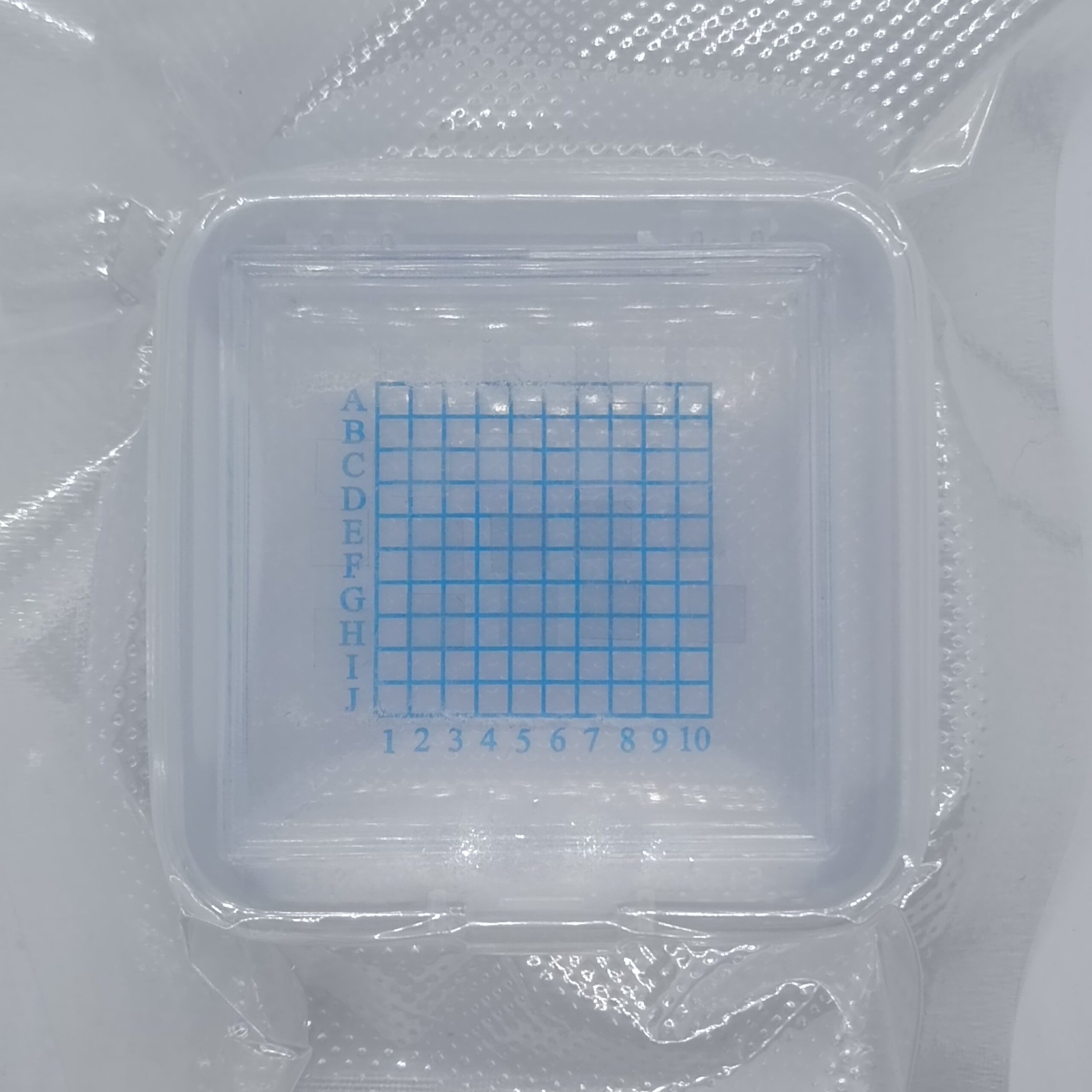
- Vacuum Gel-Pak packaging — active-side UP, preserves hydrogen-termination chemistry through global shipping.
- Laser-marked backside identification — every hydrogen-terminated diamond plate carries a unique corner mark for unit-level traceability.
Typical Specifications
| Material | Single-crystal CVD diamond, undoped |
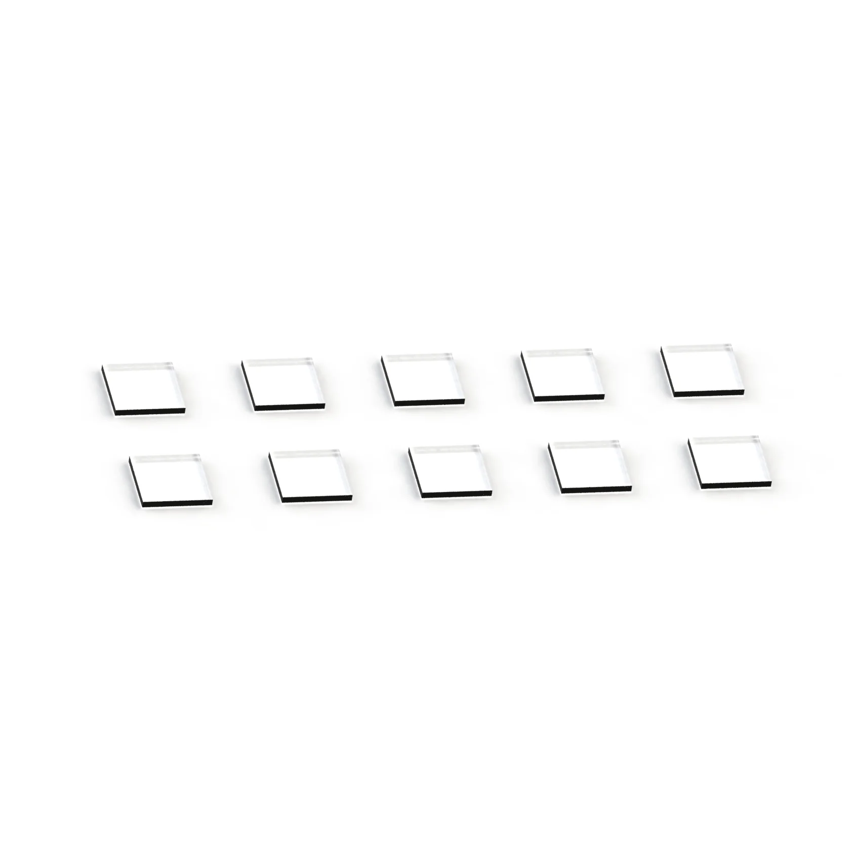
| Size | 5.0 × 5.0 × 0.3 mm (custom sizes on request) |
| Epitaxial layer | 200 nm undoped diamond, homoepitaxial step-flow growth |
| Surface termination | As-grown hydrogen (top epitaxial surface) |
| Surface roughness | Ra ≤ 1 nm (epitaxial side) |
| Identification | Laser mark on backside corner; vacuum-sealed Gel-Pak, active-side UP |
Applications
- Power MOSFETs — high-temperature, high-frequency diamond electronics.
- 2D material heterostructures — graphene-on-diamond, hBN-on-diamond devices.
- Quantum sensing — NV-center substrates and biosensing.
- High-electron-mobility transistors (HEMTs) — III-N/diamond hybrid stacks.
- UV photodetectors — solar-blind detectors on intrinsic diamond.
Process Compatibility
The 5×5 mm footprint and 0.3 mm thickness of each hydrogen-terminated diamond plate are compatible with common sample stages used in MPCVD systems, e-beam evaporators, scanning probe instruments, and benchtop optical setups. The single-crystal substrate is mechanically robust; standard diamond-tipped tweezers or vacuum wands are sufficient for handling. AFM, SEM, Raman, and photoluminescence characterization are all supported without additional sample preparation.
Packaging and Handling
Each hydrogen-terminated diamond is laser-marked on the backside (undoped-layer corner) for unit-level traceability and packaged active-side UP in vacuum-sealed Gel-Paks. The hydrogen termination is stable under vacuum storage; for ex-situ use, we recommend transferring to your process chamber within 30 minutes of Gel-Pak opening to preserve surface chemistry.
Custom and Bulk
Custom sizes (2×2 mm to 10×10 mm), thicknesses (0.1–1.0 mm), and epitaxial-layer thicknesses (50 nm – 5 µm) are available for hydrogen-terminated diamond substrates. Contact us for a quote tailored to your device geometry and target application.
Hydrogen-Terminated Diamond for Power Electronics Research
The hydrogen-terminated diamond substrate is increasingly used as the foundation for next-generation power devices that conventional silicon and silicon-carbide substrates cannot reach. Research groups are studying hydrogen-terminated diamond for high-temperature MOSFETs that operate above 300 °C, for radiation-hard detectors in high-energy-physics experiments, and for low-loss HEMT heterostructures that combine the wide bandgap of diamond with high-mobility III-N channels. The as-grown hydrogen surface lets the hydrogen-terminated diamond act as both the mechanical substrate and the device-quality interface, removing one of the most stubborn yield-killers in wide-bandgap device fabrication.
If your research program is moving toward diamond electronics or 2D-material integration on diamond, our hydrogen-terminated diamond substrate provides a benchmark-quality starting surface with traceable provenance and reproducible packaging. We support custom research orders from a single plate to multi-wafer pilot runs.
References
- Single Crystal CVD Diamond Plate — parent catalog item.
- Diamond — Wikipedia.


Reviews
There are no reviews yet.