Description
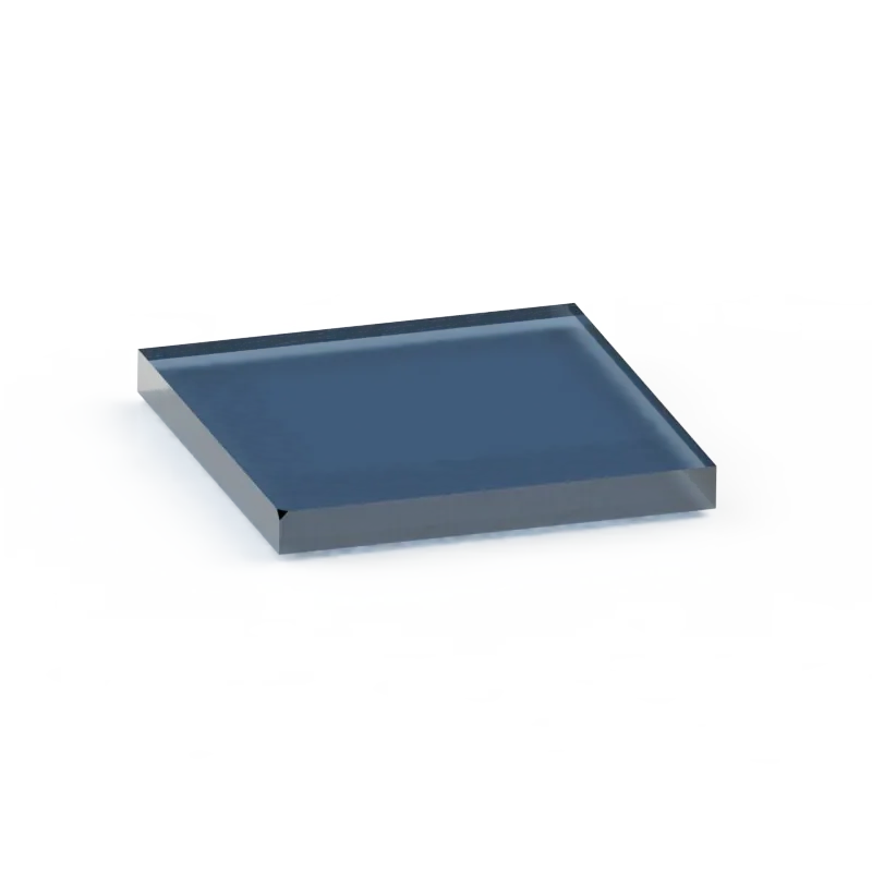
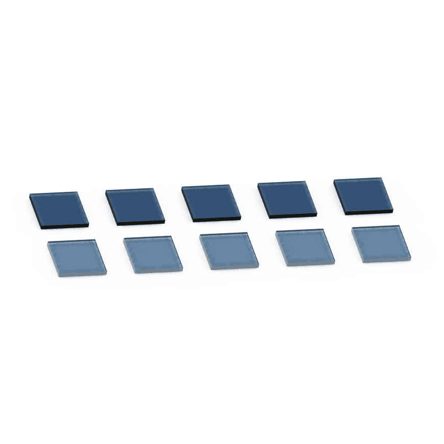
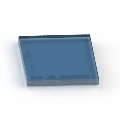
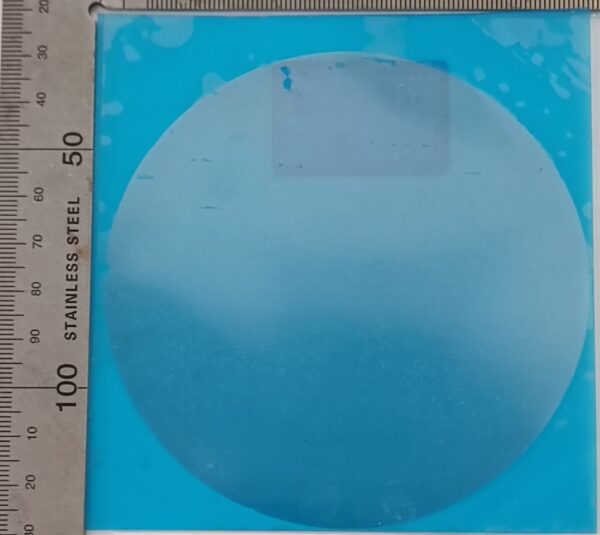
Diamond Epitaxial Wafer for MOSFET
Looking for a cutting-edge solution to elevate your power electronics? Our Diamond Epitaxial Wafer for MOSFET is here to revolutionize your designs. With unmatched thermal conductivity, durability, and performance, this wafer is engineered for the most demanding applications. Whether you’re working on electric vehicles, renewable energy systems, or high-frequency devices, this wafer is your go-to choice.
Table of Contents
Specifications
| Parameter | Value |
|---|---|
| Base Undoped Diamond Layer | 500 ± 50 µm |
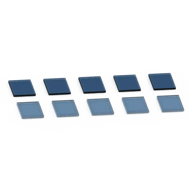
| Diamond Type | 5x5mm Single Crystal Diamond (SCD) plate |
| Heavily Boron-Doped Diamond Layer | ~0.2 µm |
| Lightly Boron-Doped Diamond Layer | ~2 µm |
Features
- High Thermal Conductivity: Diamond’s thermal conductivity surpasses silicon, ensuring efficient heat dissipation in high-power applications.
- Wide Bandgap: Enables operation at higher voltages and frequencies, ideal for advanced MOSFET designs.
- Superior Mechanical Strength: Diamond’s hardness ensures durability in extreme environments.
- Customizable Options: Available in various sizes and doping concentrations to meet your specific needs.
- Enhanced Breakdown Voltage: Perfect for high-voltage applications, ensuring reliable performance under stress.
Applications
Our Diamond Epitaxial Wafer for MOSFET is versatile and can be used in:
- Power MOSFETs: Ideal for high-power switching applications.
- High-Frequency Devices: Enables efficient signal amplification in communication systems.
- Electric Vehicle Systems: Enhances performance and reliability in EV power electronics.
- Renewable Energy: Perfect for solar inverters and wind turbine systems.
- Quantum Computing: Supports stable qubit operations in quantum devices.
- Radiation Sensors: Withstands high radiation environments, making it suitable for nuclear applications.
- High-Temperature Electronics: Operates reliably in environments up to 300°C.
Benefits
- Efficiency: Low power loss and high switching speeds.
- Durability: Resistant to heat, radiation, and mechanical stress.
- Customization: Tailored to your specific requirements.
- Future-Proof: Supports next-generation technologies like quantum computing and renewable energy.
FAQs
Q: What is the lead time for this product?
A: The standard lead time is 1 month unless otherwise stated.
Q: Can I customize the doping concentration?
A: Yes, we offer customizable doping concentrations to meet your specific needs.
Q: Is this wafer suitable for high-temperature applications?
A: Absolutely! The wafer can operate reliably in environments up to 300°C.
Q: How does this compare to silicon wafers?
A: Diamond wafers offer superior thermal conductivity, wider bandgap, and higher durability compared to silicon.
Why Choose Us?
At 6CCVD, we specialize in high-quality diamond wafers tailored for cutting-edge applications. Our boron-doped diamond products are trusted by industry leaders for their reliability and performance. Explore our polycrystalline CVD diamond wafers for more options.
External Resources
For more insights into diamond wafers and their applications, check out these resources:

Reviews
There are no reviews yet.